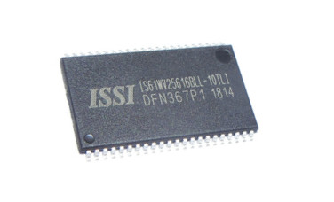
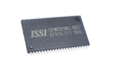
IC CHIP SRAM IS61WV25616BLL-10TLI Memory IC Chip - Asynchronous Memory IC 4Mb Parallel 10ns TSOP44
FEATURES:
HIGH SPEED: (IS61/64WV25616ALL/BLL)
• High-speed access time: 8, 10, 20 ns
• Low Active Power: 85 mW (typical)
• Low Standby Power: 7 mW (typical) CMOS standby
LOW POWER: (IS61/64WV25616ALS/BLS)
• High-speed access time: 25, 35, 45 ns
• Low Active Power: 35 mW (typical)
• Low Standby Power: 0.6 mW (typical) CMOS standby
• Single power supply
— VDD 1.65V to 2.2V (IS61WV25616Axx)
— VDD 2.4V to 3.6V (IS61/64WV25616Bxx)
• Fully static operation: no clock or refresh required
• Three state outputs
• Data control for upper and lower bytes
• Industrial and Automotive temperature support
• Lead-free available
FUNCTIONAL BLOCK DIAGRAM:
DESCRIPTION
The ISSI IS61WV25616Axx/Bxx and IS64WV25616Bxx
are high-speed, 4,194,304-bit static RAMs organized as 262,144 words by 16 bits. It is fabricated usingISSI's high- performance CMOS technology. This highly reliable pro- cess coupled with innovative circuit design techniques,
yields high-performance and low power consumption de- vices.
When CE is HIGH (deselected), the device assumes a standby mode at which the power dissipation can be reduced down with CMOS input levels.
Easy memory expansion is provided by using Chip Enable and Output Enable inputs, CE and OE. The active LOW Write Enable (WE) controls both writing and reading of the memory. A data byte allows Upper Byte (UB) and Lower Byte (LB) access.
The IS61WV25616Axx/Bxx and IS64WV25616Bxx are packaged in the JEDEC standard 44-pin TSOP Type II and 48-pin Mini BGA (6mm x 8mm).
DC ELECTRICAL CHARACTERISTICS (Over Operating Range)
VDD = 3.3V + 5%
| Symbol |
Parameter |
Test Conditions |
Min. |
Max. |
Unit |
| VOH |
Output HIGH Voltage |
VDD = Min., IOH = –4.0 mA |
2.4 |
— |
V |
| VOL |
Output LOW Voltage |
VDD = Min., IOL = 8.0 mA |
— |
0.4 |
V |
| VIH |
Input HIGH Voltage |
|
2 |
VDD + 0.3 |
V |
| VIL |
Input LOW Voltage(1) |
|
–0.3 |
0.8 |
V |
| ILI |
Input Leakage |
GND £ VIN £ VDD |
–1 |
1 |
µA |
| ILO |
Output Leakage |
GND £ VOUT £ VDD, Outputs Disabled |
–1 |
1 |
µA |
Note:
1. VIL (min.) = –0.3V DC; VIL (min.) = –2.0V AC (pulse width < 10 ns). Not 100% tested.
VIH (max.) = VDD + 0.3V DC; VIH (max.) = VDD + 2.0V AC (pulse width < 10 ns). Not 100% tested.
DC ELECTRICAL CHARACTERISTICS (Over Operating Range)
VDD = 2.4V-3.6V
| Symbol |
Parameter |
Test Conditions |
Min. |
Max. |
Unit |
| VOH |
Output HIGH Voltage |
VDD = Min., IOH = –1.0 mA |
1.8 |
— |
V |
| VOL |
Output LOW Voltage |
VDD = Min., IOL = 1.0 mA |
— |
0.4 |
V |
| VIH |
Input HIGH Voltage |
|
2.0 |
VDD + 0.3 |
V |
| VIL |
Input LOW Voltage(1) |
|
–0.3 |
0.8 |
V |
| ILI |
Input Leakage |
GND £ VIN £ VDD |
–1 |
1 |
µA |
| ILO |
Output Leakage |
GND £ VOUT £ VDD, Outputs Disabled |
–1 |
1 |
µA |
Note:
1. VIL (min.) = –0.3V DC; VIL (min.) = –2.0V AC (pulse width < 10 ns). Not 100% tested.
VIH (max.) = VDD + 0.3V DC; VIH (max.) = VDD + 2.0V AC (pulse width < 10 ns). Not 100% tested.
DC ELECTRICAL CHARACTERISTICS (Over Operating Range)
VDD = 1.65V-2.2V
| Symbol |
Parameter |
Test Conditions |
VDD |
Min. |
Max. |
Unit |
| VOH |
Output HIGH Voltage |
IOH = -0.1 mA |
1.65-2.2V |
1.4 |
— |
V |
| VOL |
Output LOW Voltage |
IOL = 0.1 mA |
1.65-2.2V |
— |
0.2 |
V |
| VIH |
Input HIGH Voltage |
|
1.65-2.2V |
1.4 |
VDD + 0.2 |
V |
| VIL(1) |
Input LOW Voltage |
|
1.65-2.2V |
–0.2 |
0.4 |
V |
| ILI |
Input Leakage |
GND £ VIN £ VDD |
–1 |
1 |
µA |
| ILO |
Output Leakage |
GND £ VOUT £ VDD, Outputs Disabled |
–1 |
1 |
µA |
Note:
1. VIL (min.) = –0.3V DC; VIL (min.) = –2.0V AC (pulse width < 10 ns). Not 100% tested.
VIH (max.) = VDD + 0.3V DC; VIH (max.) = VDD + 2.0V AC (pulse width < 10 ns). Not 100% tested.
AC TEST CONDITIONS
| Parameter |
Unit |
Unit |
Unit |
| |
(2.4V-3.6V) |
(3.3V +10%) |
(1.65V-2.2V) |
| InputPulseLevel |
0Vto3V |
0Vto3V |
0Vto1.8V |
| Input Rise and Fall Times |
1V/ ns |
1V/ ns |
1V/ ns |
| InputandOutputTiming andReferenceLevel(VRef) |
1.5V |
1.5V |
0.9V |
| OutputLoad |
See Figures 1 and 2 |
See Figures 1 and 2 |
See Figures 1 and 2 |

 Your message must be between 20-3,000 characters!